|
UBM
Tech-Insights has
recently started its
analyses
of Intel's new 22nm
process used in the
production of Ivy
Bridge. Some early
results are already
made public. We
eagerly await more
results and we also hope
to see some 22nm
process analyses
from Dick
James when he
gets his hands on an
Ivy Bridge sample..
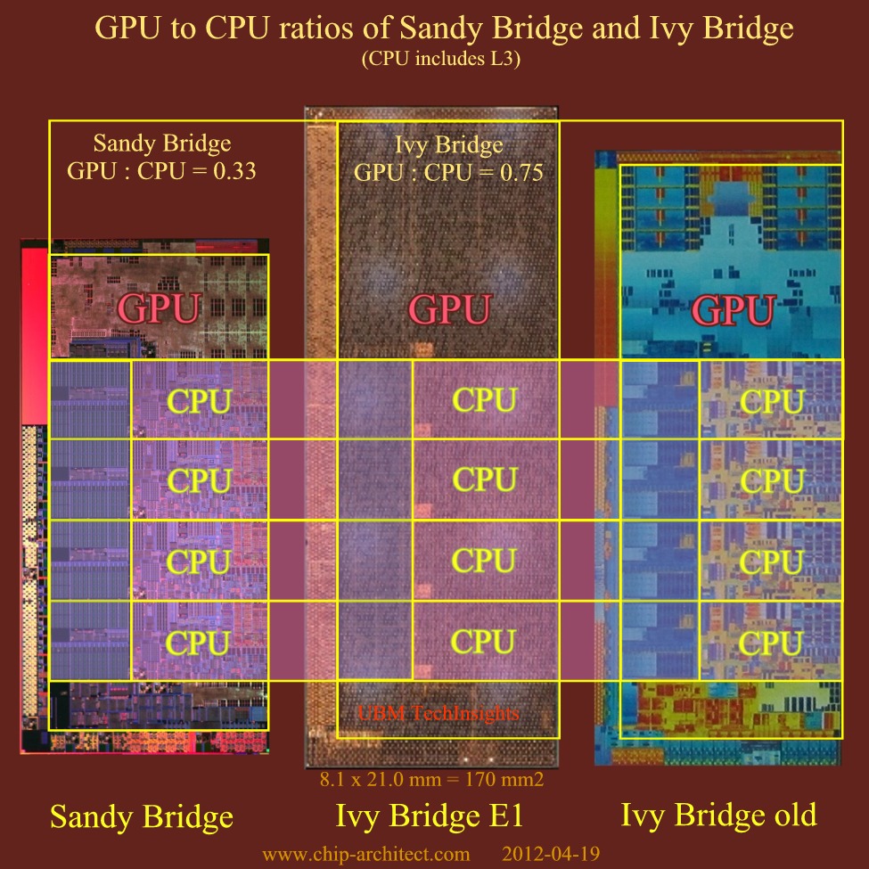
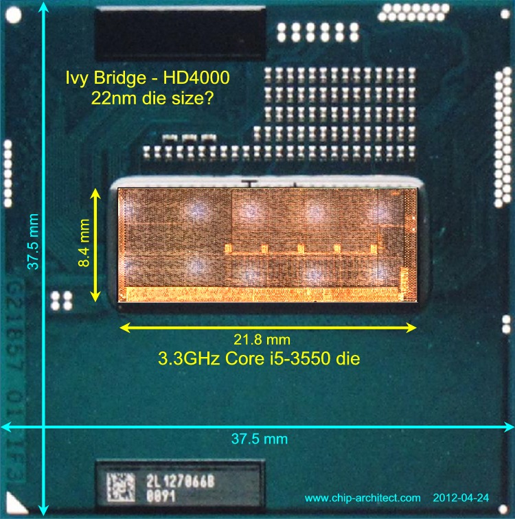
Interesting is the
die size of the
latest E1 stepping
which is the one
which will go on
sale later this
month. The surprise
is that it is
somewhat larger as
earlier steppings as
shown by Intel
itself. In the
image you can say
the die photo shown
a while ago while
the one in the
middle is the die
used by UBM. The
analyst mentions a
die size of 170 mm2
while earlier
reports estimated
160 mm2.
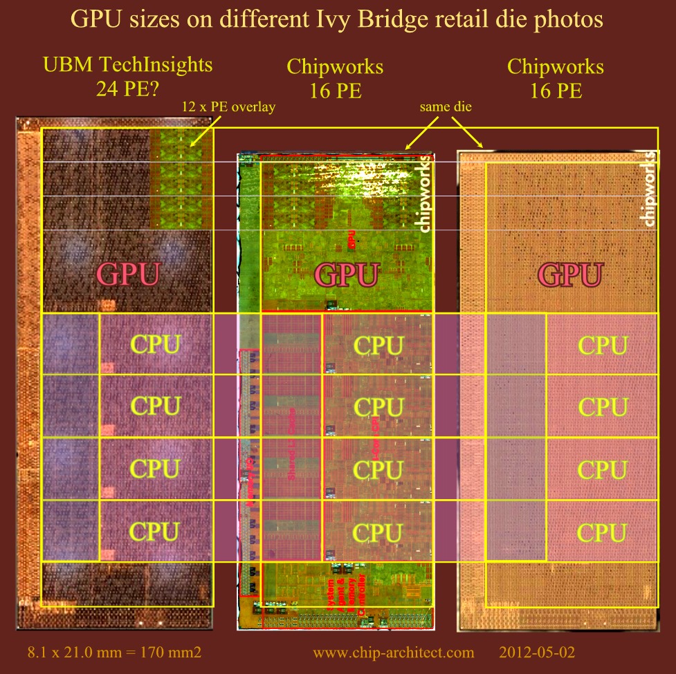
The picture from UBM
shows the upper
layer of the chip
which is enough to
figure out
whereabouts of the
most important
units. It is
clear that the GPU
has further
increased in size
compared with
earlier versions.
All in all, The
GPU-CPU ratio has
now increased to 75%
Clearly,
Sandy Bridge's GPU
performance is
generally
acknowledged to be
wholly inadequate.
The significant
increase shows that
Intel has understood
this. Some of the
increase will
improve quality
while the rest
should increase
performance. The
graphics performance
of AMD's new Trinity
APU will still be
out of reach but it
will be interesting
to see how both
compare in real
world performance.
The reviews of both
will be out in the
coming weeks.
|