|
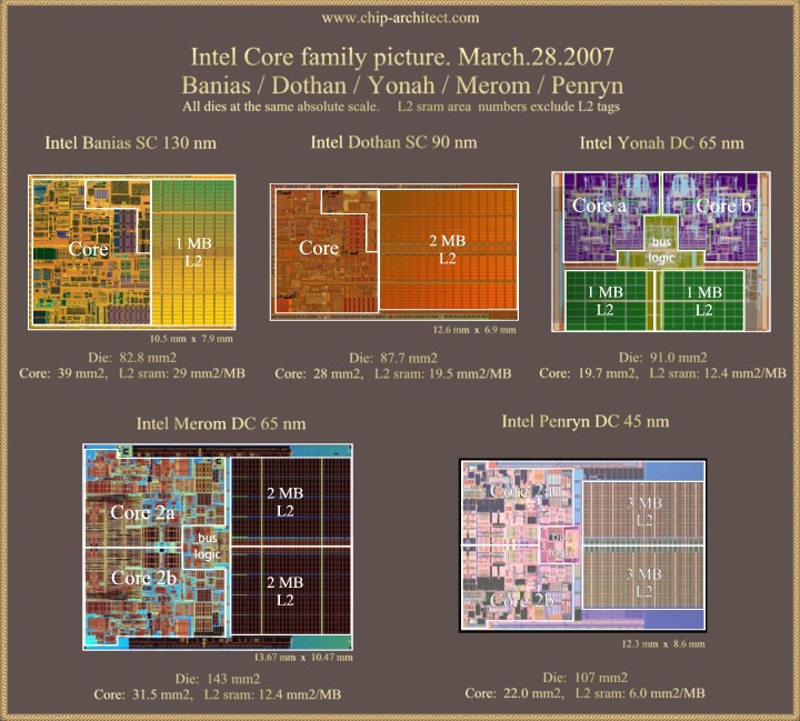
Meet
the family ! The fifth member, Penryn, has just been born
and will start walking in Q1, 2008. A few interesting
facts can be derived by comparing the different generations.
Four process node generations and two micro-architectural
generations. The
relative
scaling for the process nodes is given in the table below.
large
version
Ideal
and actual scaling during process node transitions.
|
.
|
130
nm to 90 nm
transition |
90
nm to 65 nm
transition |
65
nm to 45 nm
transition |
|
Ideal
Area Scaling |
0.48 |
0.52 |
0.48 |
|
Logic Area Scaling |
0.72 |
0.70 |
0.70 |
|
SRAM Area Scaling |
0.67 |
0.64 |
0.48 |
Die,
Core and Cache Sram areas.
|
.
|
Processor |
Die
Size |
Core
Size |
L3
/ L2 Cache Sram |
|
45
nm |
Intel
Penryn |
107
mm2 |
22.0
mm2 |
6.0
mm2 / MB |
|
65
nm |
AMD
Barcelona |
283
mm2 |
25.5
mm2 |
11.2
- 12.1 mm2 / MB |
|
65
nm |
AMD
Brisbane |
126
mm2 |
20.8
mm2 |
18.5
mm2 / MB |
|
65 nm |
Intel
Merom |
143
mm2 |
31.5
mm2 |
12.4
mm2 / MB |
|
65 nm |
Intel
Yonah |
91
mm2 |
19.6
mm2 |
12.4
mm2 / MB |
|
90 nm |
AMD
Windsor |
220
mm2 |
31
mm2 |
35.0
mm2 / MB |
|
90 nm |
Intel
Dothan |
87.7
mm2 |
28
mm2 |
19.5
mm2 / MB |
|
130
nm |
AMD
(Hip7) |
194
mm2 |
55
mm2 |
68.5
mm2 / MB |
|
130
nm |
Intel
Banias |
82.8
mm2 |
39
mm2
|
29
mm2 / MB |
updated
March 28, 2007
|