|
Hammer goes for the performance crown ( by Hans de Vries ) Fred Weber finally presented the first overview of the Hammer architecture. Exactly two years after the initial presentation at the MPF 1999. His SpecInt 2000 indication may be the ultimate proof that the AMD architects made the right decisions during the design of the Hammer: More than twice the SpecInt performance of the highest number published today, The 2 GHz Pentium 4. (http://www.specbench.org) A white paper can be found here: http://www.amd.com/us-en/assets/content_type/white_papers_and_tech_docs/Hammer_architecture_WP_2.pdf The slides from the MPF 2001 presentation can be found here: http://www.amd.com/us-en/assets/content_type/DownloadableAssets/MPF_Hammer_Presentation.PDF And
some Hammer FAQ's: http://www.amd.com/us-en/Corporate/VirtualPressRoom/0,,51_104_2315_3931,00.html To put the Hammer's SpecInt performance into perspective: The following list is assembled from the published data (white numbers), new data from MPF 2001 (yellow numbers) and finally some extrapolated numbers (red) compiled list of published and extrapolated specint 2000 scores.
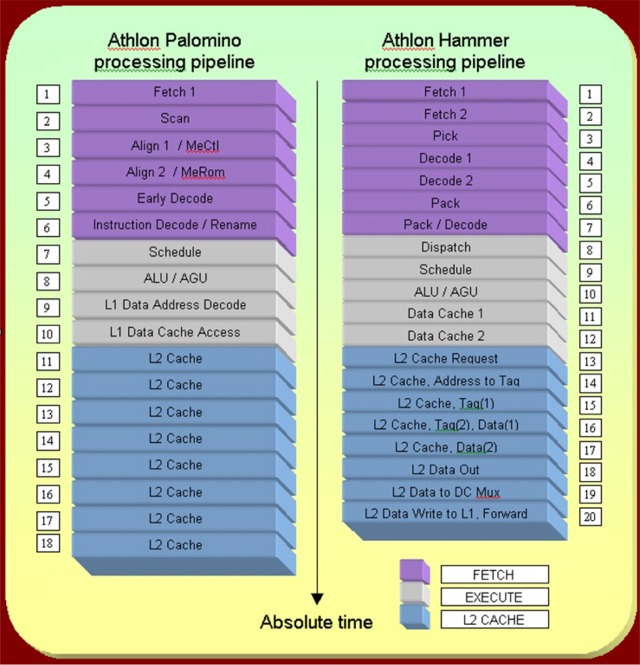
The Hammer is not based on the set of patents that we discussed a few weeks ago. These patents belong to an earlier K8 design which has been either abandoned or is possibly continued in one way or another for a future design. The currently presented Hammer resembles much more a highly tuned version of the Athlon Palomino. The Integer Processing pipeline is extended from 11 to 13 stages. The floating point pipeline is now 17 stages. (see the white paper) The rumor of an addition of two pipeline stages has been around for a while for the "Mustang/Palomino" core. It now turns out to be the Hammer core. Below we compare the Integer/L2 pipelines of the Athlon Hammer and the Athlon Palomino:
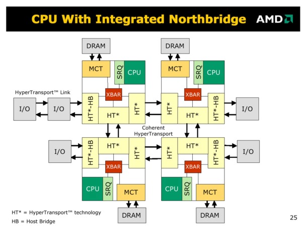
8th generation memory hierarchy and multiprocessing architecture. The Athlon has often been called a 7th generation processor with a 6th generation memory subsystem. The Hammer changes this radically. The 128 bit DDR2700 memory interface offers a 2.5 times higher bandwidth (5.33 GB/s) and a greatly reduced latency. The memory pipeline has become an integral extension of the processor pipeline. All latency other then that from the DDR SDRAM memory will scale down with the processor cycle time for subsequent generations. The three Hyper Transport links offer a combined bandwidth of not less then 19.2 GB/s. Each link has a 16 bit input channel and a 16 bit output channel all running at a dazzling speed of 1.6 GHz. Memory accesses, CPU requests and Hyper Transport packets are all routed through the 32 GB/s on chip crossbar. The design supports an optional second CPU on the die.
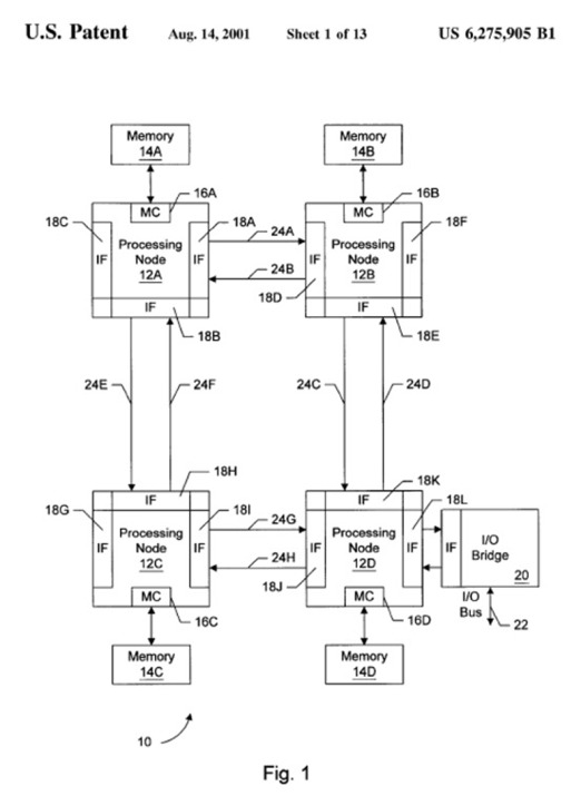
Using information from patents.... Is not always a good way to predict a processors architecture... :^) Very interesting maybe from a pure technical viewpoint but difficult to relate to actual products. One patent based prediction we made however turned out to be exactly right. Look at the text and compare figure 1 of the patent below with the drawing of presentation above.... A recently issued AMD Patent (6,275,905) on the name of Dirk Meyer and Jim Keller gives a possible system solution for an 8 way Sledge Hammer multiprocessing system. Such a system would contain four SledgeHammers each with two cores. Each SledgeHammer has its own memory controller on chip and three Hyper Transport busses. Two of these link to other SledgeHammers forming a rectangle with a SledgeHammer on each corner. The third bus interfaces each processor to its local I/O slots.
It shows that patents may contain very relevant information after all. The question is which patents do and which don't. With more information available now we may browse a bit more through AMD's patent portfolio and produce an article about Hammers architecture that goes a bit further then the presentations slides of the MPF 2001. Don't expect anything very soon however since I've got to do this all in the little bit of spare time I have beside a very busy job. Regards, Hans
|