| number: | model | date filed: | AMD's Hammer patents |
| 6,266,763 | K8-2 | Jan, 5 '99 |
Physical rename register for efficiently storing floating point, integer, condition code, and multimedia values |
| 6,256,721 | K8-1 | Jun, 16 '00 |
Register renaming in which moves are accomplished by swapping tags |
| 6,247,106 | K8-2 | Jul, 27 '00 |
Processor configured to map logical register numbers to physical register numbers using virtual register numbers |
| 6,240,503 | K8-1 | Nov,12'98 | Cumulative lookahead to eliminate chained dependencies |
| 6,230,262 | K8-2 | Jul, 31'98 | Processor configured to selectively free physical registers upon retirement of instructions |
| 6,219,784 | K8-1a | Nov,16'98 | Processor with N adders for parallel address calculation |
| 6,212,623 | K8-2 | Aug,24'98 | Universal dependency vector/queue entry |
| 6,212,622 | K8-2 | Aug,24'98 | Mechanism for load block on store address generation |
| 6,199,154 | K8-1a | Jun,19'98 | Selecting cache to fetch in multi-level cache system based on fetch address source and pre-fetching additional data to the cache for future access |
| 6,167,506 | K8-1a | Apr,23'98 | Replacing displacement in control transfer instruction with encoding indicative of target address, including offset and target cache line location |
| 6,141,747 | K8-2 | Sep,22'98 | System for store to load forwarding of individual bytes from separate store buffer entries to form a single load word |
| 6,134,649 | K8-1a | Apr,23'98 |
Control transfer indication in predecode which identifies control transfer instruction and an alternate feature of an instruction |
| 6,122,727 | K8-2 | Aug,24'98 | Symmetrical instructions queue for high clock frequency scheduling |
| 6,122,656 | K8-2 | Jul,31'98 | Processor configured to map logical register numbers to physical register numbers using virtual register numbers |
| 6,119,223 | K8-2 | Jul,31'98 | Map unit having rapid misprediction recovery |
| 6,112,293 | K8-1a | Jul,14'98 | Processor configured to generate lookahead results from operand collapse unit and for inhibiting receipt/execution of the first instruction based on the lookahead result |
|
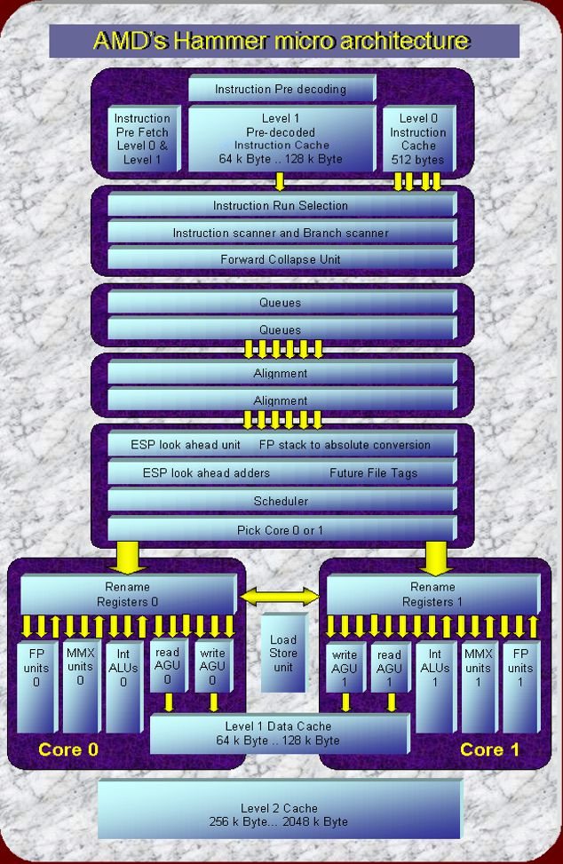
The Hammer The Hammer diagram above shows a very wide super-scalar processor. Innovative new units like the "ESP Look Ahead unit" and the "Forward Collapse unit" should help to extract an unprecedented level of instruction level parallelism from the good old X86 instruction architecture to feed all the hungry functional units. The pipeline supports not less then six instructions in parallel, twice as much as the current Athlon. It contains a double core. Both cores are loaded with functional units to execute the instructions. Some might argue that the amount of Instruction Level Parallelism in X86 code is limited and that wide super-scalar, highly pipelined architectures can not increase the performance anymore. The extra functional units simply hang in there idle. These arguments are based on theoretical studies that count the ILP in a wide range of programs. The Hammer may want to prove otherwise. The theoretical studies for instance consider the processor cycle and the operations as "atomic": The smallest possible units. The hardware designer however works with Gates and Gate-delays, significantly smaller units. Some dependent instructions might start only one or two gate delays after each other, meaning that they all may be executed in the same cycle with the right hardware, effectively in parallel.... This is for instance the case in the ESP Look Ahead Unit that allows among other things that consecutive PUSHes and POPs to and from the stack can be executed simultaneously! Furthermore, a processor may increase IPL by collecting some statistical information during run time and apply this to increase ILP. This is how the Forward Collapse Unit together with the Branch Predictor can increase ILP by effectively removing up to 2 conditional branches per cycle from the instruction stream. Most innovations in the Hammer are intended to make it the X86 processor with the highest Instruction Level Parallelism yet and should make it a very powerful single thread processor. There is no explicit talk of SMT (Simultaneous Multi Threading) in any of the patents. A processor like this one "screams" however for an SMT inplementation. SMT gives chip-architects the ideal excuse to continue on the line of wider and wider super scalar processors and higher and higher super pipelined processors, beyond the level that would be economically feasible for single thread processors. Further on we do a bit more SMT speculation of our own. below we discuss the various stages of the micro architecture shown in the diagram Instruction fetch and scanning Instruction queuing and aligning Chip-Sets and Multi Processing
|
|
AMD's Hammer Micro Architecture: Instruction fetch & scanning
Two levels of instruction cache. The single cycle latency Level 0 cache can provide up to four cache lines each cycle while the large multi-cycle Level 1 cache provides one line just as it does in the Athlon. The Level 0 cache serves two purposes: It allows the Level 1 instruction cache to grow because it can compensate the higher latency in many cases. It also allows the branch prediction unit and the branch history table to grow: Branch prediction: "going both ways before deciding on the prediction" The Level 0 cache simultaneously provides the code that has to executed when a conditional branch is taken as well as the code that has to be executed if the branch is not taken. The processor goes "both ways" for a moment until the large branch prediction unit has had the time to make a decent decision. In some cases the result of the branch prediction is effectuated several cycles after the instructions are loaded from the level 0 cache: The "forward collapse unit" that is some 3 stages further down the line handles short forward branches where the branch and the destination address in the same "run" of code. The instructions that are skipped if the branch is taken are marked as canceled in this stage. The "forward collapse unit" can handle up to two short forward branches per cycle to handle these nested "if-then-else-statements" which are usually responsible for this type of code. Increasing Instruction Level Parallelism by "removing" conditional branches. The effect is that more instructions per cycle can be handled. Branches typically reduce ILP (instruction Level Parallelism) because subsequent instructions depend on the outcome of the condition. The Hammer should be able to extract more ILP from the instruction stream then any compiler would be able to find. Actually more then the theoretical maximum that a compiler would be able to extract. The difference is that a compiler can only remove conditional branches from the code when it can predict them with 100% accuracy. Units like the "forward collapse unit" can "remove" up to 2 conditional branches per cycle from the instruction stream in cooperation with the branch predictor that also can predict up to 2 conditional branches per cycle! Branch prediction: "remembering instead of re-learning" A huge 64k entry branch history table is used for branch prediction. The "taken/not taken" results of the 16 latest conditional branches are used to calculate an index in the 64k table. The table contains 65536 2 bit bimodal counters that hold the predictions: 0 strongly not taken, 1: weakly not taken, 2 weakly taken, 3: strongly taken. Such a large table can store the characteristic branch patterns of many different branches in a larger program without much interference. A smaller table has to re-learn the branch pattern again when it comes back to recently executed code. A very large table still holds valid information even when the processor has been executing other code for a while. And a larger table can also be more accurate then a smaller one. Up to two branches may be predicted per cycle. Instruction pre-decoding: Support for handling branches Each byte in the instruction caches has 2 bit of pre-decode information. AMD has looked at many different ways of pre-decoding sometimes with much more then two bits. The final scheme chosen is shown in the table below. - definition of the pre-decoding bits -
Pre-decode bit 1 identifies the byte as the Start byte of an instruction. The instruction can then either be a branch or a non branch instruction depending on pre-decode bit 0. It is important to identify branches early to get the Pre-fetch unit to load new instructions as soon as possible. A second innovation are the pre-computed branch addresses of 8 bit and 32 bit relative displacements. The instruction cache does not contain the displacements anymore but the absolute addresses instead. The address calculations are done only once when the instructions are loaded in the instruction cache instead of each time the instruction is executed. |
|
AMD's Hammer micro architecture: Instruction queuing & aligning
The Instruction Queue: Delivering up to six instructions per cycle The instruction queue receive runs of instruction byte including those bytes that have been marked as cancelled by the forward collapse unit because they are predicted to be skipped over by short forward branches. The instruction queue select up to six instructions cycle within up to four runs of instructions and present them to the alignment unit, skipping the cancelled instructions. The Alignment unit: The alignment unit is configured to route the instructions bytes belonging to the up to six instructions selected by the instruction queue to an equivalent number of issue positions from where they will be fully decoded. |
|
AMD's Hammer micro architecture: Rename and schedule unit
The Look Ahead unit: A novel way to extract more parallelism from the X86 IA The X86 instruction set is different compared to others in that it has very view registers. More memory accesses are therefore needed. Furthermore, these memory accesses are for a large part made with the aid of special purpose registers: The Stack Pointer (ESP) and the Base Pointer (EBP). This in contrast with a RISC processor that can use any of it's registers for memory address calculation. It is this limitation that is turned into an advantage in the Hammer with the ESP Look Ahead unit. The look ahead unit owns it name to the fact that it pre-executes some operations simultaneous to the decoding of instructions, long before the instructions enter the Out-Of-Order execution pipeline. It co-operates with a future (register) file that indicates if an x86 register is still valid if all preceding instructions still in the pipeline are executed. The current implementation chosen for the Hammer concentrates on operations using the ESP register: The Stack Pointer. This special purpose register will typically change often but the new stack pointer value can in many cases be determined during instruction decoding. Instructions that add an immediate value to the stack pointer like PUSH; POP; ADD ESP, IMM; can be handled in parallel. So-called "constant generators" determine the constants to be added to the stack pointer for up to six stack instructions per cycle. It can do this in parallel because the time it takes to add six values together takes hardly more time then it takes to add only two numbers. A technique called "Carry-Save-Addition" is used here. This technique is also used in multiplier hardware that implement multiplication by adding many values in parallel. So up to six different ESP values can be calculated per cycle for consecutive stack operations. Advantage 1: Increased Instruction Level Parallelism. The ESP look ahead unit Increases Instruction Level Parallelism, multiple PUSHes and POPs can be executed simultaneously. Other X86 functions that modify the Stack Pointer and that can be accelerated with the ESP Look Ahead unit are: CALL; RET 0,N; PUSH; POP; ADD ESP, IMM; ENTER 0,N; LEAVE 0,N; MOV EBP,ESP; and MOV ESP,EBP. Advantage 2: Reduced effective Load Latency of the Data Cache. Memory Loads can be performed earlier on. Succeeding instructions that depend on these loads perceive this as a reduced load latency of the Level 1 Data Cache. Advantage 3: Relaxed Load / Store Ordering. It resolves memory conflicts before memory accesses are scheduled. Out of Order architectures can be seriously hampered because Loads have to wait until Store addresses of preceding Stores are resolved. These Stores might overwrite the memory locations that are about to be Read. The Look Ahead unit resolves these memory conflicts at the earliest possible moment during decoding when the instructions are still in order. Architectures like the EV6 and the Pentium 4 predict if a store address is equal to the read addresses of any closely following loads. The entire pipeline is restarted if a miss-prediction occurs and the load was executed out of order before the store. The hammer patents do not mention such a mechanism for AMD's next generation processor but the look ahead unit provides a different type of solution.
|
|
AMD's Hammer micro architecture: The Dual Cores
The Dual cores of the Hammer. Before speculating on Simultaneous Multi Threading (SMT) which is not explicitly mentioned in the patents we will discuss the Dual Cores from the classical single thread viewpoint. Both cores have their own register sets with renamed registers for out of order processing. A communication mechanism between the two takes care that the contents of both stays equal. It takes an extra cycle for a result to be propagated from one register file to the other. AMD looked at taking this down to a 1/2 cycle but probably concluded that the benefits did not match the trouble. This concept looks a lot like the EV6 that also has two instances of its register file. One combined register file with enough ports to serve all available functional units simply becomes to big and tends to slow down the cycle time. A single thread can take advantage of all available functional units in both cores whenever sufficient parallelism can be extracted from the program. Picking the Core. An interesting issue is how divide the instruction stream over the two cores. Two diametrically opposite strategies are described in earlier patents. The "K8-1a" alternates between cores on an instruction base. So even instructions would go to core 0 and odd instructions would go to core 1 for example. This has a serious disadvantage because the extra cycle delay between the two cores will occur very often. The "K8-2" on the other hand sends a "line" of multiple instructions to one core and then a line of instructions to the other core and so on. This reduces the penalty for extra cycle latency but may limit the parallelism. The latest patents do not mention a specific method anymore. We expect that the Hammer may now use a distribution method that looks at the data dependencies to decide which core should be picked on an instruction base. A simple strategy would be to pick the core where the instruction operands become available first and where the type of execution unit needed is still available. SMT speculations. There are basically two ways to implement Simultaneous Multi Threading on the dual core Hammer architecture. The first method would allow instructions of different threads to use both the cores just like in the case of single threaded operations. This method would allow the maximum level of parallelism but would increase the penalty of the extra cycle latency caused by communication between the two cores. More communication between the cores is needed. The second method would split two threads over the two cores so that each thread has its own core. This limits the maximum amount of parallelism but eliminates the extra cycle communication cycle latency. The second method may show a higher performance in the general case where programs have a limited amount of parallelism. A further advantage of the second method may be when the two different threads are from two different programs. In this case each thread needs it's own complex X86 memory management and protection context. Both cores have there own memory ports so a different context may be stored in each of the two cores. It is much more interesting to have a processor that can execute two different programs simultaneously then one that can execute two different threads from the same program with one identical context. There is a very big difference between these two cases implementation wise. X86-64. The dual cores support 64 bit processing. AMD made the bold move to go it alone and not wait for Intel to implement a 64 bit X86 extension with an extended register set. Intel may now be forced to develop something similar forced by the Hammer with the risk of jeopardizing its Itanium and McKinley series of processors. The sheer size of both the Pentium 4 and the McKinley make a hybrid solution that has both on the same die unfeasible as a solution that provides both 64 bit functionality and top speed compatibility in a way the Hammer does.
|
|
AMD's Hammer micro architecture: Chip-Sets and Multi Processing
ClawHammer: 266 MHz EV6 bus replaced by 800 MHz Hyper-transport. A number of ClawHammer chipsets have now been placed on the roadmaps. These chipsets use Hyper Transport to communicate with ClawHammer at a presumable speed of 800 MHz and a total bandwidth of 6.4 Giga Byte/s. Three times that of the current 266 MHz EV6 bus. Hyper Transport is said to scale to 1.6 Giga Hertz and 12.8 Giga Byte/s. The Memory Controller is still integrated on the Chipsets with support for 266 and 333 MHz DDR SDRAM. One should hope that these chipsets support 128 bit busses to memory to take advantage of the higher bandwidth. SledgeHammer for 2 to 8 way multiprocessing A recently issued AMD Patent (6,275,905) on the name of Dirk Meyer and Jim Keller gives a possible system solution for an 8 way Sledge Hammer multiprocessing system. Such a system would contain four SledgeHammers each with two cores. Each SledgeHammer has its own memory controller on chip and three Hyper Transport busses. Two of these link to other SledgeHammers forming a rectangle with a SledgeHammer on each corner. The third bus interfaces each processor to its local I/O slots.
|
|
Some background info behind this article: - Non of it is based on any advanced Micro Processor Forum sheets. - Most of it is based on the Patents mentioned - ClawHammer has no on chip memory controller: Based on the public roadmaps of VIA/SIS see: http://www.viahardware.com/roadmap02_3.shtm It mentiones that the K8T333 and K8M333 use 266-333 MHz DDR memory. - The processor is not assembled by me from many different patent bits and pieces. -The entire processor from Instruction cache to retirement is described as a whole in the patents -The patents describe the entire processor in some detail and then focus on a particular issue -A number of Athlon Patents described an entire processor with many similarities to the Athlon -My drawing is based on the drawings in the patents. -Most Athlon patents are from 1996 (file date) -The Patents that I used are mostly from 1998 -Patents are not always a good base to predict a micro processor. -Specially numbers used in Patents can be different from the numbers in an actual processor -Numbers should be interpreted as ?in the order of? instead of exact values. -The Sledgehammer I/O (memory controller + 3x HT) is speculative and based on another patent mentioned in the Article. - Dual Core capabilities have been mentioned by AMD on various occasions (to start with Fred Weber MPF 1999) - The combination of various AMD marketing material and graphics has lead many to assume that a 2 GHz Hammer would be about 3 times as powerful as a 1 GHz Athlon. This would imply a huge increase in Instruction level parallelism. One can only hope to achieve something like this by adding ?scores? of ILP improving innovations. - But it is well possible that the name ?Hammer? has been moved to an entire different processor like a Palomino with X86-64 and Hyper transport for instance. -The Clawhammer processor in the article would not fit that easy in 105 mm2. It would limit 1 level caches to 64 kB both and the 2nd level cache to 256 kB like in the current Palomino. The high speed and low latency of HT would help however. But then, the Clawhammer is the ?Duron? of the Hammer family. -We hope to get some detailed information on October 15 from the Micro Processor Forum although it is unclear what exactly will be presented there.
|
![]()
![]()