|
Motorola/AMD HiP7: The good news and the bad news
The good news so far is that the next process jointly developed by AMD and Motorola seems to be an absolute world class process which will include both SOI and a low k dielectric with a k lower then 3.0 So far only IBM announced such a process for 2001 and HiP7 doesn't trail by more than six months or so. The Hammer family will be based exclusively on this 130 nm SOI process. The SOI and low-k features may give it a raw 30% speed advantage over it's large competitor Intel, significantly more then it has now with it's copper process that gives AMD a 10% to 15% advantage.
The bad news is that the transition to 130 nm it's still a while away. Surprisingly little is know what AMD's plans with the Palomino core are until then. There have been a number of road-map changes lately. The Mustang with it's big cache has disappeared and the 1.5 Ghz Palomino version has been delayed from January 2001 to Q2 2001. It looks that AMD has recently made it's mind up about what it is going to do in the mean time. It may be that 130 nm production with 248 nm KrF laser scanners did not turn out to be reliable enough to reach sufficient high yields. A remark was made that at AMD analyst meeting that it may use 193 nm ArF scanners for some parts of it's 130 nm process although the HiP7 presentation still mentions 248 nm for all layers. (Only the most critical layers need the latest equipment) The recent revelation of the SOI version of Motorola's G4+ codenamed Apollo in HIP6 (180 nm) opens the possibility of an SOI variant of the 180 nm Palomino which would increase performance by 25% or so and or reduce power consumption for mobile versions. The Mustang with up to 1 Megabyte of cache may be considered simply to big for an 180 nm process and AMD may wait for Big Cache processors until the 130 nm Hammer family. __
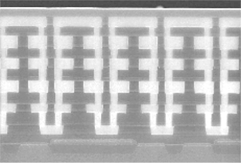
HiP7: Up to 9 layers of copper separated by a low k dielectric. Source: Motorola Motorola's and AMD's 130 nm HiP7 CMOS process can support up to 9 layers of copper with two options for a low k dielectric. (k=3.7 and k<3.0) Copper reduces the wire resistance by 40% over Aluminum. A low-k with a k smaller then 3.0 dielectric reduces the amount of current which has to flow into the wire to change the voltage from a logical '0' level to a logical '1' level by 30% thereby improving the wire delay with the same percentage. Ongoing Research & Development
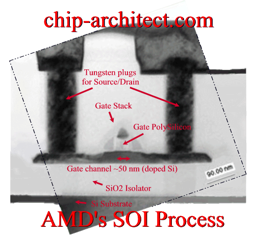
A few impressive slides during AMD analyst meeting reveal future process directions. The transistor above shows a drawn gate length of ~50 nm (Lpoly). The effective gate length can be even shorter depending on the exact doping profile in the Gate channel.
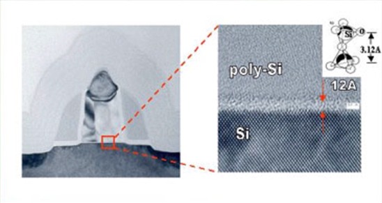
The gate oxide which isolates the Gate terminal channel which connects the Source and the Drain is a mere 1.2 nm thick (12 Å) The image on the right shows the individual atoms. The crystalline Silicon has a very regular pattern in contrast with the poly-crystalline Silicon. The Silicon Dioxide layer separating the two is much smaller than the 2.0 nm that was considered to be the theoretical minimum only 2 years ago. ..
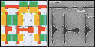
Alternating Phase Shift Mask for thin Gates. Source: AMD Extremely thin gates like the 50 nm gates and below can be produced with the help of Phase Shift Masks. The red masks are the usual binary masks. The results shown on the left show the distortions caused by the laser wavelength (248 nm) which is much longer then the projected details. These distortions can be improved with OPC (see below). The picture above shows the alternating phase shift masks as yellow and green. The phase of the coherent laser light is shifted in opposite directions. This method allows the creation of well defined extremely thin lines in the border region between them. These thin lines are typically used to define the transistor Gate which separates the transistor Source and Drain. The smaller the separation the higher the switching speed. Optical proximity Correction: Source: MaskTools The 'blurbs' caused by the Optical Proximity effects can be partly corrected by adding Serifs and Scattering Bars (shown black) to the original binary masks. The "Low Pass Filter effect" is more or less reversed by applying a "high pass filter" to the Mask. The Serifs have the effect of sharpening the corners. The above OPC mask is produced with Mask Rigger. A software product of Mask Tools (ASML group) and used by companies like IBM, TSMC and likely AMD as well for their 130 nm processes. We'll get some more information on the HiP7 process after December 12 from the San Francisco IEDM 2000 presentation: http://www.his.com/~iedm/techprogram/index.html (See section 23) |

![]()
![]()