|
Two consecutive presentations during this years International
Electron Device Meeting in San Francisco on December 12 will reveal details about the next generation 130
nm processes that Intel and AMD plan to use to continue their ongoing micro-processor speed race.
AMD will jointly present their co-developed 130 nm process with Motorola. AMD and Motorola will use ASML's 248 nm
lithography tools which means that AMD should be able to ramp up volume production
well before Intel which will use SVLG's 193 nm scanners. The Intel process
looks more aggressive on the design rules while AMD and Motorola are out
in front in terms of interconnect. Motorola/AMD's use of a low k (<3.0) dielectric used to
isolate the wires comes as a real surprise. IBM was until now the only one to apply such
a low k-dielectric (Silk, k=3.0) which should decrease wire delays in a similar way as
copper does. The question is if AMD will use this option from the start or begin
with the more conservative FSG (fluorosilicate glass) method that uses basically
fluor doped SiO2. The use of a real low-k dielectric was the third
major break-through for IBM after copper and SOI. The big mystery around AMD is where SOI fits
in. This combined Motorola/ AMD presentation shows the close cooperation
between the two. Motorola recently disclosed how it developed the
SOI G4+ PowerPC processor (codenamed Apollo) during this years Micro processor Forum
and an SOI AMD processor may be closer then held possible only a few months ago
although I would not expect anything before H2 2001.
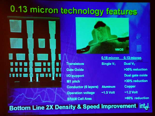
Update: Intel has
now announced that the gate oxide for the fast transistors will be a mere 1.5
nm! The small 2.45 um2 SRAM cell size will shrink even further to 2.09 square
micron. This is 2.7 times smaller as the current SRAM cells used in the PIII and
P4. The overall speed of the 130 nm process will be 65% faster then that of the
current 180 nm process! The 'vote' is still out what the Motorola/AMD SRAM cell
size concerns but we expect it to be even smaller then the future 2.09 square
micron from Intel based on previous Motorola processes and the use of
local interconnect. http://www.intel.com/pressroom/archive/releases/cn110700.htm
Update: (Nov 9th) AMD has now announced that it will use an SOI process in H2 2001 ! The use of an insulator underneath the Si transistors (Silicon On Insulator) provides a frequency improvement of 22-30% and is therefore twice as significant for the processor performance as the addition of copper wires. The addition of a low K dielectric (k<3.0) would further increase this to 30-38%.
IEDM 2000 program
Intel Developers Forum, Fall 2000. from www.watch.impress.co.jp/pc IEDM, San Francisco, Tuesday, December 12, 3:10 p.m. 23.3 A 130nm Generation Logic Technology Featuring 70nm Transistors, Dual VT Transistors and 6 layers of Cu Interconnects, S. Yang, P. Bai, T. Bramblett, B. Crew, M. Hussein, P. Jacob, C. Kenyon, B. Mcintyre, P. Moon, S. Sivakumar, B. Tufts, S. Thompson, S. Tyagi and M. Bohr, Intel Corporation A leading edge 130nm technology with 6 layers
of Cu interconnects for high performance dense logic is presented.
Aggressive design rules and unlanded contacts offer a 2.45um2 6-T
SRAM cell using 248nm lithography. A highly manufactorable 2.4nm
electrical gate oxide with dielectric time to fail that meets the requirements
for 1.2V operation including tolerances is presented. Dual threshold
voltage devices are offered to maximize product performance at acceptable
product standby current.
Motorola / AMD 130 nm process IEDM, San Francisco, Tuesday, December 12, 3:35 p.m. 23.4 A Versatile 0.13 µm CMOS Platform Technology Supporting High Performance and Low Power Applications, A.H. Perera, B. Smith, N. Cave, M. Sureddin, S. Chheda, R. Singh, M. Celik, S.-C. Song, D. Wu, A. Sultan, J. Chang, R. Islam, K.C. Yu, R. Fox, S. Park, F. Tolic, C. Simpson, S. Crown, D. Eades, S. Gonzales, S. Venkatesan, V. Kolagunta, C. Nelson, J. Sturtevant, D. Bonser, N. Benavides, M. Kling, M. Thompson, V. Sheth, J. Fretwell, S. Kim, N. Ramani, K. Green, D. Pham, M. Moosa, P. Besser, Y. Solomentsev, D. Denning, M. Friedemann, B. Baker, R. Chowdhury, R. Mikkola, S. Ufmani, K. Strozewski, R. Carter, J. Reiss, M. Olivares, B. Ho, T. Lii, T. Sparks, T. Stephens, M. Schaller, C. Goldberg, K. Junker and D. Wristers, Motorola DigitalDNA Laboratories and AMD, Austin, TX A high performance 0.13 mm CMOS technology has
been developed with process modules allowing its usage as a plat-form for
a wide range of applications, from GHz microprocessors to low power mobile
ICs with non-volatile memory. Three core devices are provided in combination
with 50 or 70Å DGO MOS- FETs for the I/Os. Optical enhancement techniques
with 248 nm lithography tools provide the patterning capability for gate
lengths from 110 to 80 nm. Dual and single inlaid copper metalization allow
9 levels of
|