An analysis of the newly presented
Pentium 4 core.
Ample information
The new Pentium 4 core micro architecture contains
many interesting aspects. There is however very little detailed information
given by Intel. Here I try to fill the void with a detailed analysis.
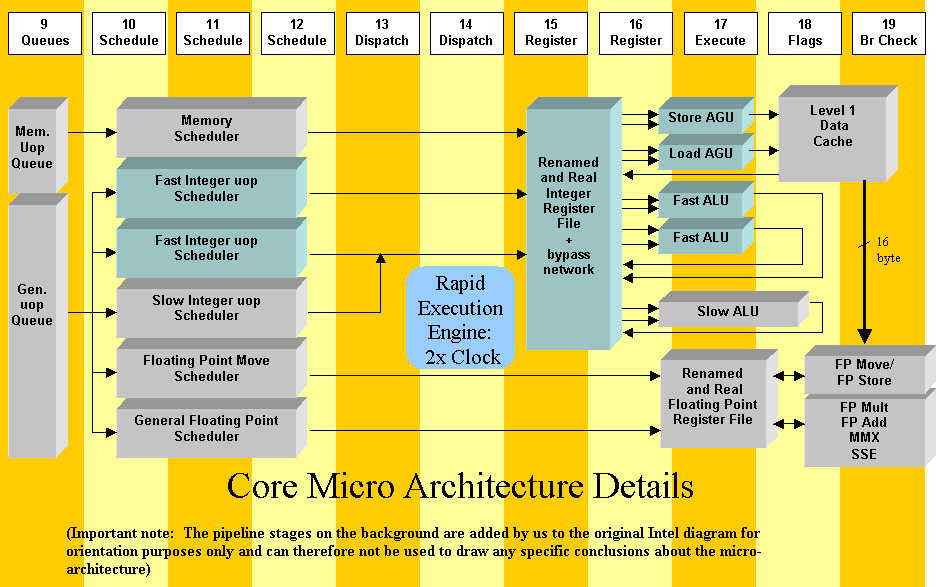
A car pool lane for memory loads
Stage nine of the Pentium 4 contains the queues
where instructions line up and are waiting for further processing. The
diagram shows a separate queue for memory instructions that gives memory
loads a car pool lane on the Pentium 4 micro architecture highway that
allows them to pass the other instruction traffic. This is essential since
each instruction ultimately depends on some data loaded from memory. It
is important to execute the loads as early as possible, also because loads
can incur significant delays in case of cache misses.
Load-Load reordering
Stages 10 to 12 contain a separate Memory Scheduler
for the loads. This means that loads can be issued in a different order
then the program order. This is useful since not all loads can be issued
in advance. A load may depend on the value of a register that is still
unknown. The scheduler can use the addressing mode as a clue for load-load
re-ordering. Loads which can typically be executed well in advance are
those that use the base pointer together with an immediate offset given
by the instruction itself. A modern compiler will avoid pops and pushes
to access the stack. Instead it may use the base-pointer with immediate
displacements like EBP+4 or EBP-8. Accesses into structures with
EDI+disp or EDI+disp are also good candidates. A structure is often accessed
multiple times so the compiler can try to keep the pointer in the register
constant for a while. Loads with complex address modes like Base+shift*Index+displacement
should be scheduled as last because they are dependent on so many registers.
The actual availability of the data in the register
file needed may also be used as a clue for load scheduling. There are quite
a few stages between the start of the scheduler and the register file however
so it maybe too early on in the pipeline to be very useful. Maybe it is
used in the last part of the scheduler that is closer to the register file.
Load-Store reordering
The memory stores also follow the separate queue/scheduler
path. Reordering loads and stores is a very different story however and
it is unlikely that the Pentium 4 can do this. The point is that the memory
addresses are still unknown during scheduling so a load following a store
may read from the same memory address that the store wants to write. Loads
are therefor scheduled in program order with stores. Stores are not reordered
with other stores either for the same reason. This kind of reordering would
require speculative processing much like the speculative processing after
a branch prediction. If the direction of the branch is predicted wrong
then all speculative instructions must be canceled and the pipeline must
be restarted. If turns out that a load rescheduled for a store has provided
the wrong memory data then all dependent instructions must be canceled
and restarted. (An architecture that does this is the Alpha EV6). The now
one and a half year old Athlon does not do any load-load or load-store
reordering. This is the reason that it is not very much faster then the
Coppermine even though it has a superior number of integer and floating
point units. The following pseudo code example shows how important load-store
reordering can be for floating point processing.
STORE (A*B+C) to
MEM1;
LOAD (D)
from MEM2;
The load may then have to wait ~8 cycles (Athlon)
or ~14 cycles (Pentium 4) until the floating-point calculations are finished
while MEM1 and MEM2 may be completely different addresses? Well,
this problem is solved for a large part in the Load/Store unit. This unit
is directly coupled to the L1 Data Cache RAM and Address Generator Units.
The dispatcher issues the load and the store without waiting for the floating-point
result. The load and the store would end up in the Load/Store unit where
the addresses are calculated. The Store may then say to the Load: "Hey
guy, you can go now. I probably have to wait quite a while for my floating
point result data from the FP move/store unit but we now know that we have
different addresses".
This doesnt handle any speculative load-store
reordering however and loads still have to wait for the store addresses.
About 37% of the x86 instructions contains a load while 23% contains a
store. (Link)
Some instructions contain both. This means that any Out Of Order x86 processor
is severely limited in its abilities to reorder code without speculative
load-store reordering. Finally: Shared memory and memory mapped I/O constitutes
a problem for both load-load and load-store reordering. Any processor needs
to have the operating system hooks to handle these issues.
The Instruction schedulers.
Stage 9 of the pipeline also shows a large general
instruction queue. I expect that it is actually divided in to several smaller
queues connected to the five different schedulers shown in stages 10 to
12. Here we encounter the first double frequency units of the Rapid
Execution Engine: The two Fast-Integer-uop schedulers. Each scheduler serves
a double frequency ALU. It can accept two uops per cycle from the queue.
The first uop is handled directly while the second starts half a cycle
later. These schedulers have a total of 6 pipeline stages running on the
double clock frequency. They handle additions, subtractions, increments,
decrements and boolean functions. Then there is the Slow-Integer-uop scheduler.
It handles other integer instructions like shifts, bit-field functions
and a lot of legacy functions like decimal and ascii adjust. It runs at
the normal frequency has three pipeline stages and can accept 1 uop per
cycle. The Slow-Integer-uop functions are handled by the Slow ALU that
also runs at the normal frequency.
The floating-point schedulers may be longer then
three stages. This would explain why the FP register file is drawn farther
to the right in the original Intel block diagram. Floating point scheduling
is more complex because the floating-point execution units have many stages.
The fact that the x87 instructions are stack based should not be an issue
anymore because the register-stack-to-renamed-register-re-mapping is already
handled in the rename stages before the queue stage.
Load data speculative execution
This is a new feature in the Pentium 4 core.
Instructions that depend on load data from the L1 data cache are scheduled
and dispatched to coincide with the arrival of the data from the L1 data
cache. These instructions are tracked, canceled in case of a cache miss
and later replayed to coincide with the arrival of the valid data. Only
the instructions dependent on the load data are replayed, independent instructions
are allowed to complete. The Alpha EV6A has a similar feature.
The double frequency register
file.
This file contains both the real x86 integer
register set and the renamed registers which are used for speculative execution.
The renamed registers can be retired to the real registers when it sure
that the branch direction chosen by the branch prediction unit was the
right one and that the speculative results of the renamed registers are
valid. The register file runs also runs at the double frequency and thus
contains 4 pipeline stages. It would have been possible to run the register
file at the normal frequency but with twice the number of data ports.
This however would have made the register-file four times bigger. The Intel
designed team therefor decided to give it extra pipeline stages instead.
Interesting is that the Elbrus design team uses this method to limit the
size of the huge combined Integer / Floating point register file of their
E2K processor. This seems much more achievable now that Intel does the
same.
The double frequency ALUs
The double frequency ALUs where already disclosed
during the Spring IDF. The 2 ALUs can together execute 4 operations per
cycle. This however is the not reason of their design. (Four operations
per cycle is overkill compared to the number of load/store ports of the
cache) Much more important is that they can do back to back additions
and subtraction as well as boolean functions with an effective latency
of ½ a cycle. This can significantly speed up serial code.
We still dont believe that they can complete a full 32 bit addition within
½ a cycle. We suspect that the ALU uses CSA (Carry Save Adder)
methods to reach an effective latency of an ½ cycle. This means
that the ½ cycle does not apply to all cases: An additive function
followed by a boolean function would still see a full cycle latency. (This
full cycle latency can indeed be found in the Spring IDF presentation).
There is another latency issue that is not immediately visible in the block
diagram. The x86 instructions use implicit flags like zero, sign, parity
et-cetera. These flags are calculated in stage 18 and then they are forwarded
together with the result data to the Bypass network and the Integer register
file. This means that operations that depend on result data from another
ALU may see a latency of 2 cycles instead of 1 cycle. This is probably
the reason that shifts are relatively slower than on the P6.
The double frequency AGUs
The AGUs are a part of the Rapid Execution Engine
and also run at the double frequency. This is somewhat puzzling since the
MPF presentation explicitly shows that the L1 data cache runs at the normal
speed. A reasonable explanation might be that the total Load-Use latency
of the L1 data cache (AGU+RAM access) is 2 ½ cycles. This might
be reduced to an effective latency of 2 cycles if the preceding operation
is an additive function (add, subtract, increment, decrement). This is
exactly the case in the example used during the Spring IDF presentation.
The same CSA method that is probably used in the ALUs can combine the
additive function with the address generation and thereby cut ½
a cycle from the total latency. The worst case latency can be 3 cycles
in this case. This happens when the preceding function is not an additive
function and the result becomes available in the wrong ½ cycle (The
last ½ cycle of the normal clock) Vias Centaur team uses
the same CSA method in their recent designs.
For so far a more detailed technical analysis
of the newly presented Pentium 4 core micro architecture.
Send your comments to: hansdevries@chip-architect.org
HOME
|